How to Avoid too much Solder on your RF PCB
When RF circuits operate at high frequencies of 50+ GHz, every single piece of extra metal impacts impedance of the tightly controlled traces. We look at how to ensure just the right solder on the RF PCB Advanced printed circuit boards (PCBs) are so complex, that OEMs often scratch their heads and wonder if they are going down the right path with their PCB assemblies. With many challenges for their specific board applications, not all assembly houses are equipped to deal with one key area, the radio frequency (RF) PCB.
When an RF circuit operates at a high frequency, such as 50+ GHz, every single piece of extra metal on the board impacts the impedance of the tightly controlled traces. This can impact return loss and reflection, but may also cause other signal integrity issues.
This becomes even more critical when PCBs are made with standard FR-4 or FR-6 type PCB material rather than more expensive RF-qualified material, such as polytetrafluoroethylene (PTFE) or Astra MT77.
Also, grounding voids are critical to RF PCBAs. IPC-A-610 leaves the final acceptance criteria for the large ground pads under QFN-type parts to be agreed between the OEM and the contract manufacturer (CM). IPC does specify acceptance of 30% voids on collapsed BGA solder ball with much less solder volume.
In the case of OEMs producing RF PCB designs, their goals in this regard can be less than 25% (even less than 10% in some cases) voiding on large ground pads under QFN-type parts. Less than 25% or less than 10% voiding is possible only with proper assembly procedures.
Beyond grounding voids, five key PCB assembly areas that demand the closest OEM attention are component selection, PCB material selection, stencil design, reflow profile, and functional test.
Component Selection
Component selection requires close attention to not only consider signal integrity requirements but also assembly requirements. The design engineer must understand assembly challenges when selecting a package. If the end result can be achieved with less challenging packages, then the design engineer must select those packages.
Examples of active component packages could be flip-chip versus micro BGA or a QFN-type package and passive parts could be 0201-sized passives rather than 01005-sized passives, especially the capacitors. Challenges associated with these components are further discussed below.
PCB Material Selection
PCB material and finish play key roles in the final trace impedance. PCB houses are unable to manage demands of high-frequency circuit requirements with FR-4, PTFE, Astra MT77, or a hybrid of FR-4 and PTFE type materials used for higher frequency PCBs.
Stencil Design
The stencil design is the linchpin for effective RF PCB assembly to avoid dispensing extra and damaging solder. When an RF circuit is operating at 50+ GHz level, every single piece of extra metal impacts the impedance of the circuits.
Trace length and impedance are critical and are tightly controlled. When PCBs are made with standard FR-4-type material, the final trace impedances must be compensated during the assembly process. The smallest amount of extra solder can result in degradation of the signal integrity of the circuit in the form of return loss and reflection.
Therefore, today’s RF board must adopt the most stringent requirements to control trace length and pad sizes along with exposing and not exposing certain traces. Exposed traces with any unintended solder not only change the impedance of the circuit but may also cause other unintended signal integrity issues, such as cross-talk and noise.
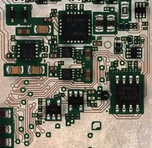
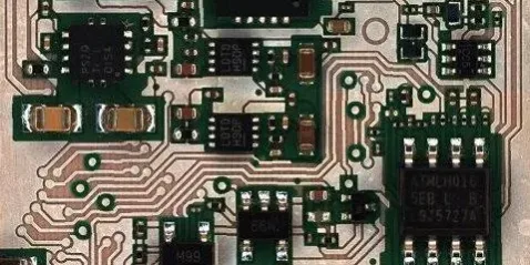
Two key points to keep in mind are, number one, that the amount of solder that is dispensed on the pads should remain within the controlled area. It cannot run onto the trace. Figure 1 shows clean traces without any solder on them.

Figure 1. The amount of solder dispensed on the pad needs to remain within the pad.
Secondly, using the bare minimum amount of solder is important, dispensing only the sufficient amount needed for a good quality solder joint. Any extra solder causes interference in the performance of the RF circuitry, as mentioned above.
Determining Correct Stencil
In many cases, EMS providers and their assembly personnel design the assembly process without collaborating with the design engineer. However, with RF PCBs, the board designer plays a critical role in determining the correct stencil for a given RF board assembly. Certain highly important aspects must be taken into consideration.
For example, he or she must clearly define device packages on the critical RF path. During the stencil design, the aperture size has to be closely considered for all parts on the critical RF path, especially packages like flip-chip, BGAs, and QFNs. Any lower or higher volume of solder can deviate the RF board’s output performance.
Pad design for certain chip types is also critical. Here, you need sufficient solder volume to achieve a good solder joint. But not more than required where there is an RF interference.

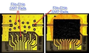
Figure 2. Flip chips have minimum solder bumping for circuit board connection.
Further, keeping the points cited above, you have to consider that newer RF circuitry chip installation requires increasingly smaller apertures. For instance, flip chips are becoming more common for RF circuitry. As shown in Figure 2, they have minimum solder bumping to connect to the circuit board, so the amount of dispensed solder becomes even less.
Solder Paste Solvents
Complementary circuitry for advanced RF chips frequently makes use of extremely tiny 01005-size capacitors. The solder volume dispensed on 01005 pads or on the small pads for flip-chip type active parts creates a unique challenge where solder volume has to remain minimum due to the RF circuits, but at the same time, solder joints must have good flow.
With smaller apertures, the volume of flux required for good flow is reduced too. Special attention must be paid on the reflow profile to get good flow with a reduced flux amount. Solder paste includes flux, which contains solvents, resins, and surfactants required for the good flow of the solder joints.
Any extra solder volume on the 01005-sized passive parts introduces the possibility of hairline bridging underneath the part. It’s worth noting that the majority of x-ray equipment, including high-resolution 5DX systems, are able to detect bridging under a resistor but not able to detect bridging under capacitors, especially 01005-size capacitors.
Consequently, the assembly house has to be sufficiently experienced to successfully install a high number of 01005 capacitors on an RF circuit to avoid potential bridging. It bears repeating here that the challenge is to have enough solder volume for a good flow, but not too much solder as to cause bridging during component placement.
Ground Voids
Another critical aspect of RF performance is good grounding. Grounding is an important aspect of high-speed RF circuits because current needs to flow through the ground to complete the loop. The chip’s bottom side is a large ground in QFN-type parts.
When reflowing a large ground area, voids of varying sizes and percentages are formed. Voids are trapped gases in the solder joints. Reducing voids is challenging, but not impossible. With careful process design, profiling, and proper stencil design, ground voids can be reduced to less than 10%.
Reflow Profile
Once the board is assembled, the reflow profile becomes highly critical. It must account for the volume of solder and the available flux to perform proper flow.
Once the solder is printed, reflow timing or the time it takes to get the board to reflow becomes critical.
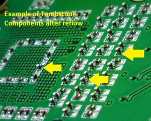
If it takes too long, some of the solvents in the solder paste on tightly controlled small pads may evaporate before even reaching the reflow system. Also, once the board is being reflowed, some challenges may arise, such as dry solder or tombstoning (figure 3) of the smaller passive devices or 01005-Size components.

Figure 3. Assembly house must be experienced to successfully install passive devices including 01005 capacitors on an RF circuit to prevent tombstoning and bridging. (Image: Courtesy of NexLogic Technologies, Inc.)
Those two challenges are exacerbated due to the limited volume of solder that is allowed to dispense on high-frequency RF circuits. All of this requires experience, the right equipment, the right tool design, and process control.
A variety of different reflow technologies can be used. Those include regular convection reflow with carefully controlled profile. Vapor phase reflow systems can be very useful, especially for a mix of very dense components with very small components on the same side. A vapor phase system with a vacuum is critical for void reduction as well. In some ways, reflow becomes more critical considering the volume of solder and the volume of the available solvents in the paste.
Functional Test
The OEM provides the information or specifications for functional testing to the assembly house. Custom functional testing on RF-type circuits is sometimes the only testing method available due to their frequency and constraints on creating test points. Test points are not prevalent on RF circuits. Hence, without test points, either flying probe or in-circuit testing is inefficient.
Therefore, functional testing of RF circuits may use a vector network analyzer (VNA) type of equipment for waveform analysis. This level of advanced functional testing requires experienced engineers, technicians, and programmers.
But it must be pointed out that functional testing has its own limitations. It cannot tell you the details of a failure. That’s why the process must be extremely stringent for RF assemblies from beginning to end. You don’t want to burden the functional tester for failure detection since it has limited to no ability to pinpoint those failures.
Summary
As we’ve said here, an RF PCB falls in the category of complex assemblies. But it is unique in the sense it demands experienced assembly floor engineering and technicians to plan and execute such critical areas as component selection, PCB materials, a correct stencil design, attention to the complementary circuitry, reflow profile, and functional testing.
Above all, the stencil must be virtually perfect to prevent extra and unnecessary solder from being dispensed onto the board. Hence OEMs searching for an assembly house for their RF PCB assembly should consider evaluating their requirements based on the assembly steps described above.


 “Shahab Jafri is the founder and president of